Introduction
Xilinx MIG (Memory Interface Generator) IP를 생성할 경우 User Logic과 연결되는 Interface는 두 가지가 있습니다.
- Standard User Interface
- AXI4 Interface
여기서는 Standard User Intrface를 control하기 위한 Design Guide를 3개의 BLOG를 통하여 설명하려고 합니다.
PC 사용환경은 다음과 같습니다.
- OS : Windows 10 pro ( version : 20H2 )
- Vivado version : 2020.2
- FPGA Part : XC7A50T-1FTG256
- DDR3 Memory Part : MT41K128M16XX-15E
Entire Design Block Diagram
앞으로 다음과 같은 Design 구현을 설명하려고 합니다.

여기서는 MIG IP의 생성과 Standard User Interface에 대한 설명, 그리고 MIG_CTRL에 구현될 FSM ( Finite State Machine )에 대하여 설명하겠습니다.
Xilinx MIG (Memory Interface Generator) IP
1.
Vivado에서 MIG IP 생성 시, Target DDR3 memory를 "MT41K128M16XX-15E"로 설정 합니다.
| Setting | Value |
| Clock Period | 3,300 ps ( 303.03 MHz) |
| Memory Type | DDR3 SDRAM |
| Memory Part | MT41K128M16XX-15E |
| Memory Voltage | 1.5V |
| Data Width | 16 |
| Data Mask | Enable |
| Input Clock Period | 4,950 ps ( 202.02 MHz, board의 실제 입력 클럭은 200 MHz 임) |
| Output driver impedance control | RZQ/6 |
| Controller chip select pin | Disabled |
| Rtt (nominaal) : on-die termination | RZQ/6 |
| Internal Vref | Enabled |
| Internal termination impedance | 50 ohms |
2.
MIG IP의 Standard User Interface는 다음과 같은 Signals가 있습니다.
| SIgnal Name | Direction | Data width (bit) | |
| Write/Read Command Signal | app_cmd | input | 3 |
| Address Signal | app_rdy | output | 1 |
| app_en | input | 1 | |
| app_addr | input | 28 | |
| Data Signal (Write Operation) | app_wdf_rdy | output | 1 |
| app_edf_wren | input | 1 | |
| app_wdf_data | input | 128 | |
| app_wdf_end | input | 1 | |
| Data Signal (Read Operation) | app_rd_data_valid | output | 1 |
| app_rd_data | output | 128 | |
| app_rd_data_end | output | 1 | |
| Clock / Flag Signal | ui_clk | input | 1 |
| ui_clk_sync_rst | output | 1 | |
| init_calib_complete | output | 1 |
3.
MIG IP를 사용할 경우에 User Logic에서 사용할 reset 을 다음과 같이 구현하면 좋습니다.
( 반드시 아래의 code를 그대로 사용할 필요는 없습니다. 개념만 보아 주세요. )
| reset <= init_calib_complete and ui_clk_sync_rst; |
4.
MIG IP의 Standard User Intrface를 control하려면 다음과 같은 FSM ( Finite State Machine )을 고려하여 설계하면 좋습니다. ( 반드시 아래의 FSM을 그대로 사용할 필요는 없습니다. )

"st_initial" state 에서는
reset = '1' 이면 current state를 유지합니다.
reset = '0' 이면 "st_idle" state로 갑니다.
"st_idle" state 에서는
app_cmd = "000" 이면 "st_write" state로 갑니다.
app_cmd = "001" 이면 "st_read" state로 갑니다.
그 외의 경우는 current_state를 유지합니다.
"st_write" state 에서는
app_cmd = "000" 이면 write operation을 하고 current_state를 유지합니다.
app_cmd ≠ "000" 이면 "st_idle" state로 갑니다.
"st_read" state 에서는
app_cmd = "001" 이면 read operation을 하고 current_state를 유지합니다.
app_cmd ≠ "001" 이면 "st_idle" state로 갑니다.
5.
Write operation과 관련된 signals는 다음과 같습니다.
| SIgnal Name | Direction | Data width (bit) | |
| Write/Read Command Signal | app_cmd | input | 3 |
| Address Signal | app_rdy | output | 1 |
| app_en | input | 1 | |
| app_addr | input | 28 | |
| Data Signal (Write Operation) | app_wdf_rdy | output | 1 |
| app_edf_wren | input | 1 | |
| app_wdf_data | input | 128 | |
| app_wdf_end | input | 1 |
아래는 Write operation의 Timing diagram 입니다.

Write operation에는 3가지 종류의 Write Timing Diagram이 있습니다. 개인적으로는 1번의 Write Timing Diagram을 선호합니다.
"app_cmd"가 "000"면 Write Operation을 진행 한다는 것입니다.
"app_rdy", "aap_wdf_rdy"가 동시에 High일 경우에 "app_en", "app_wdf_wren", "app_wdf_end"를 High로 놓고 "app_addr" (Adress), "app_wdf_data" (Data)를 drive하면 됩니다.
아래는 Evaluation Board에서 ILA IP를 사용하여 확인한 Write operation의 Timing diagram 입니다.
( 아래 그림을 클릭하면 큰 화면으로 확인할 수 있습니다. )

6.
Read operation과 관련된 signals는 다음과 같습니다.
| SIgnal Name | Direction | Data width (bit) | |
| Write/Read Command Signal | app_cmd | input | 3 |
| Address Signal | app_rdy | output | 1 |
| app_en | input | 1 | |
| app_addr | input | 28 | |
| Data Signal (Read Operation) | app_rd_data_valid | output | 1 |
| app_rd_data | output | 128 | |
| app_rd_data_end | output | 1 |
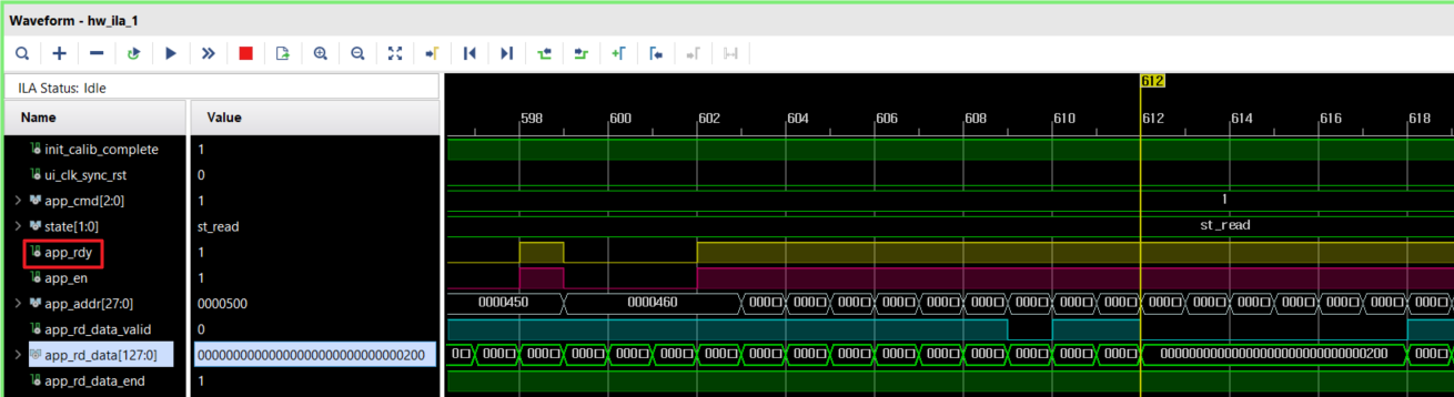
아래는 Read operation의 Timing diagram 입니다.

"app_cmd"가 "001"면 Read Operation을 진행 한다는 것입니다.
Read operation은 "app_rdy"가 High일 경우에 "app_en"을 High로 놓고 "app_addr"을 drive합니다. 이 후, "app_rd_data_valid"가 High가 되면서 "app_rd_data"가 나오는 것을 알 수 있습니다.
아래는 ILA IP를 사용하여 살펴본 Read operation의 Timing diagram 입니다.
( 아래 그림을 클릭하면 큰 화면으로 확인할 수 있습니다. )
다음은 아래 링크의 블로그를 통하여 실제 Design Code를 살펴보겠습니다.
Design Guide for MIG IP (2/3)
Introduction 아래의 Design Guide for MIG IP (1/3)을 보고 난 후, 지금 보고있는 BLOG를 보아 주세요. 여기서는 MIG IP를 Control하기 위한 MIG_CTRL ( mig_ctrl.vhd )를 design함에 있어 FS..
740280.tistory.com
저의 BLOG가 여러분의 FPGA 설계에 조금이라도 도움이 되었으면 합니다.
오늘도 좋은 하루 되세요.
(공감, 구독, 댓글은 저에게 힘이 됩니다!)
Xilinx 본사는 한국 내에 Corporate and Sales Distributor로 MAKUS를 두고 있습니다.
Xilinx 국내 Corporate and Sales Distributor인 MAKUS는 XIlinx FPGA Device를 기술영업을 통해 판매하며 기술지원이 가능합니다.
MAKUS www.makus.co.kr
Create Date: December 29, 2020
Posted By: Mouessee
관련 BLOG
Design Guide for MIG IP (2/3)
Introduction 아래의 Design Guide for MIG IP (1/3)을 보고 난 후, 지금 보고있는 BLOG를 보아 주세요. 여기서는 MIG IP를 Control하기 위한 MIG_CTRL ( mig_ctrl.vhd )를 design함에 있어 FS..
740280.tistory.com
Design Guide for MIG IP (3/3)
Introduction 만일 Design Guide for MIG IP (1/3)과 Design Guide for MIG IP (2/3)의 내용을 보지 않았다면.... 아래의 Design Guide for MIG IP (1/3)과 Design Guide for MIG IP (2/3)을 보고 난 후에..
740280.tistory.com
How to create Xilinx MIG IP for Custom Part
How to create Xilinx MIG IP for Custom Part
Introduction Xilinx 7-Series device를 사용할 경우, MIG IP를 생성할 때 선택할 수 있는 DDR2/DDR3 SDRAM Part는 모두 Micron DDR2/DDR3 SDRAM device입니다. Samsung 혹은 SK Hynix의 DDR2/DDR3 SDRAM device..
740280.tistory.com
How to create a custom csv file for MIG IP
How to create a custom csv file for MIG IP
Introduction 일반적으로 MIG IP를 사용하여 DDR4 SDRAM memory와의 Interface를 구현합니다. 하지만 MIG IP의 DDR4 SDRAM parts list에서 내가 선택한 DDR4 SDRAM part가 보이지 않는 경우가 있습니다. 내..
740280.tistory.com
'Xilinx > IPs' 카테고리의 다른 글
| How to create Xilinx MIG IP for Custom Part (0) | 2022.06.23 |
|---|---|
| MIG IP에서 사용되는 3 종류의 Clock에 대하여 (0) | 2022.05.18 |
| DisplayPort에 대한 Xilinx Solution (0) | 2022.05.16 |
| Design Guide for MIG IP (3/3) (1) | 2022.05.16 |
| Design Guide for MIG IP (2/3) (1) | 2022.05.16 |