Introduction
JTAG to AXI Master (PG174 - October 5, 2016) 라는 IP를 사용하면,
Vivado Hardware Debug Manager의 TCL console을 통하여 JTAG을 지나서, FPGA 내부 Design된 JTAG-to-AXI Master IP를 지나서, AXI Interconect( or Smart Connect)를 지나 연결되어 있는 Peripherals( BRAM, GPIO, etc... )에 Write/Read를 할 수 있습니다.

TCL console을 통하여 TCL command를 사용하기 때문에 어느 정도의 TCL language를 알고 있으면 좋습니다. 하지만 TCL language를 잘 모르더라도 여기에서 앞으로 설명하는 TCL command를 사용하는 것만으로도 그 활용도는 충분하다고 생각합니다.
나중에 시간적인 여유가 된다면 TCL language를 공부하여도 절대로 손해보는 일은 없을 것 입니다. TCL language에 대하여 보다 자세한 내용은 아래의 링크를 보아주세요.
Table of Contents
Step 1 : Example Design with JTAG to AXI Master IP
Step 2 : The Address map for the JTAG to AXI master
Step 3 : Debug Setup after Synthesis
Step 4 : Implementation, program and debug
Step 5 : TCL command for read and write in the Console
Step 1 : Example Design with JTAG-to-AXI Master IP
1.
테스트 환경은 다음과 같습니다.
| OS | Windows 10 pro (version 1909) |
| Vivado | Version 2020.1.1 |
| Board | Avnet Artix-7 50T Evaluation Board |
| Target Device | XC7A50T-1FTG256C |
간단한 Block Design과 mark_debug, Set Up Debug을 사용한 경험이 있는 User를 대상으로 합니다.
2.
아래의 링크를 클릭하면 JTAG-to-AXI Master IP를 사용한 Example Design을 download 받을 수 있습니다.
Download Link : Example Design with JTAG-to-AXI Master IP
아래의 링크를 클릭하면 Avnet Artix-7 50T Evaluation Board의 관련 자료를 확인할 수 있습니다.
Web-Site Link : Avnet Artix-7 50T Evaluation Board
3.
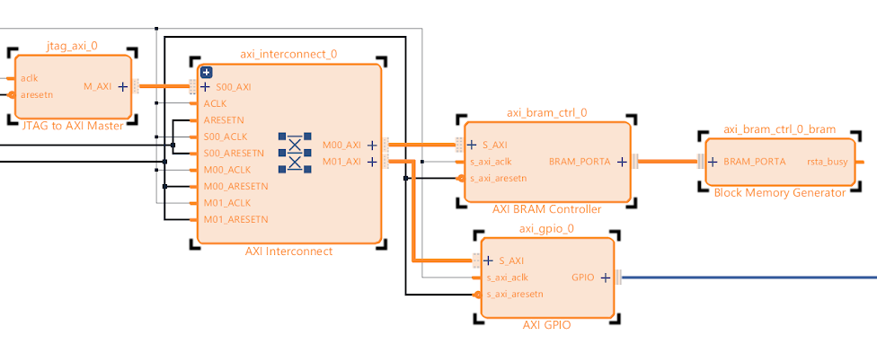
Download 받은 Example Design의 Block Design을 살펴보면 다음과 같습니다.

JTAG-to-AXI Master IP와 Peripherals만을 확대하여 보면 다음과 같습니다.
Step 2 : The Address map for the JTAG to AXI master
1.
Block Design의 "Address Editor" tap을 클릭합니다. 그리고 BRAM과 GPIO의 각 Base Address를 확인합니다.
BRAM의 Base Address는 "0xC000_0000" 입니다.
GPIO의 Base Address는 "0x4000_000" 입니다.
위 Base Address는 나중에 사용하게 됩니다.

2.
Vivado Top menu의 Flow에서 "Run Synthesis"를 클릭합니다.

Step 3 : Debug Setup after Synthesis
1.
Synthsis가 완료되면, "Open Synthesis Design"을 클릭합니다.

2.
Vivado Top menu의 Window에서 "Debug"를 클릭합니다.

3.
아래와 같이 output pin인 led[7:0]이 probing되어 있음을 확인할 수 있습니다.

이 부분은 source code의 mark_debug 그리고 Debug 창에 있는 Set Up debug를 통하여 이미 설정된 것입니다. (여기서는 mark_debug와 setup debug에 대하여 알고있는 user를 대상으로 하기 때문에 별도의 설명을 하지 않습니다.)


mark_debug에 대하여 보다 자세한 내용은 아래의 YouTube 영상을 보아 주세요.
[Xilinx] How to use Vivado Logic Analyzer : Mark Debug
Step 4 : Implementation, program and debug
1.
Implementation과 Generate Bitstream까지 완료합니다.

2.
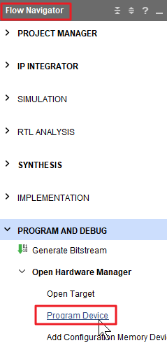
Flow Navigator에서 "Open Hardware Manager"를 클릭합니다.

3.
나타난 HARDWARE MANAGER 창에서 "Auto Connect" 아이콘을 클릭합니다.

4.
Flow Navigator 창에서 "Program Device"를 클릭합니다.
5.
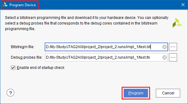
나타난 Program Device 창에서 "Program"을 클릭합니다.
6.
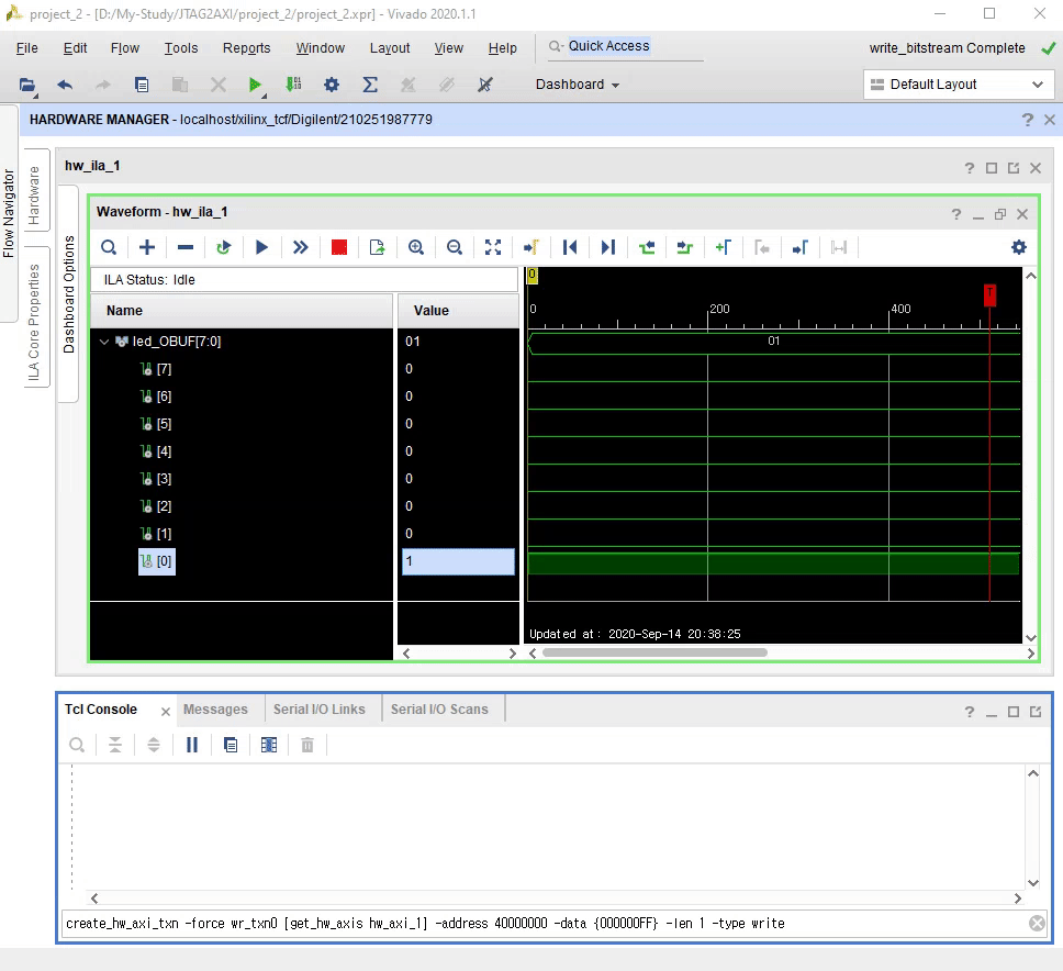
Waveform 창에서 "Run trigger immediate for this ILA core" 아이콘을 클릭합니다.
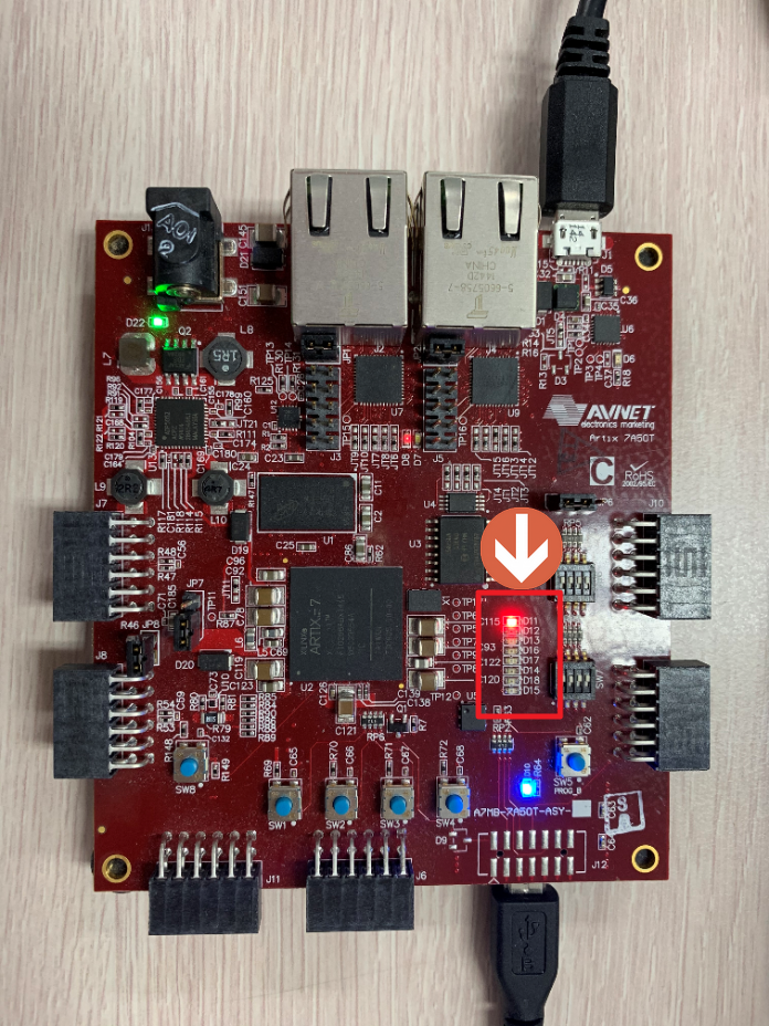
Out put pin인 led[7:0]="00000000"임을 확인할 수 있습니다.

초기에는 led[7:0]="00000000"이기 때문에 Board의 8개의 LED는 모두 "off" 입니다.

Step 5 : TCL command for write and read in the Console(1)
1.
JTAG-to-AXI Master IP를 지나서, AXI Interconect( or Smart Connect)를 지나 연결되어 있는 GPIO에 Write/Read를 하여 보겠습니다.
GPIO의 Base Address는 "0x4000_0000"입니다.
예를 들어 Address "0x4000_0000"에 Data "0x0000_0001"을 write하면 led[7:0]="00000001"이 됩니다.
예를 들어 Address "0x4000_0000"에 Data "0x0000_00FF"을 write하면 led[7:0]="11111111"이 됩니다.
2.
다음의 TCL command를 TCL console에 기입한 후, Enter합니다. (아래 Write.txt 참조)
| TCL command (Write Operation) |
| create_hw_axi_txn -force wr_txn0 [get_hw_axis hw_axi_1] -address 40000000 -data {00000001} -len 1 -type write run_hw_axi wr_txn0 |
이 후, 아래의 Animated GIF와 같이 Waveform 창에서 "Run trigger immediate for this ILA core" 아이콘을 클릭합니다.
Output pin인 led[7:0]="00000001"임을 확인할 수 있습니다.

Output pin인 led[7:0]="00000001"이므로 Board의 8개 LED 중 하나의 LED만 "on"됩니다.
3.
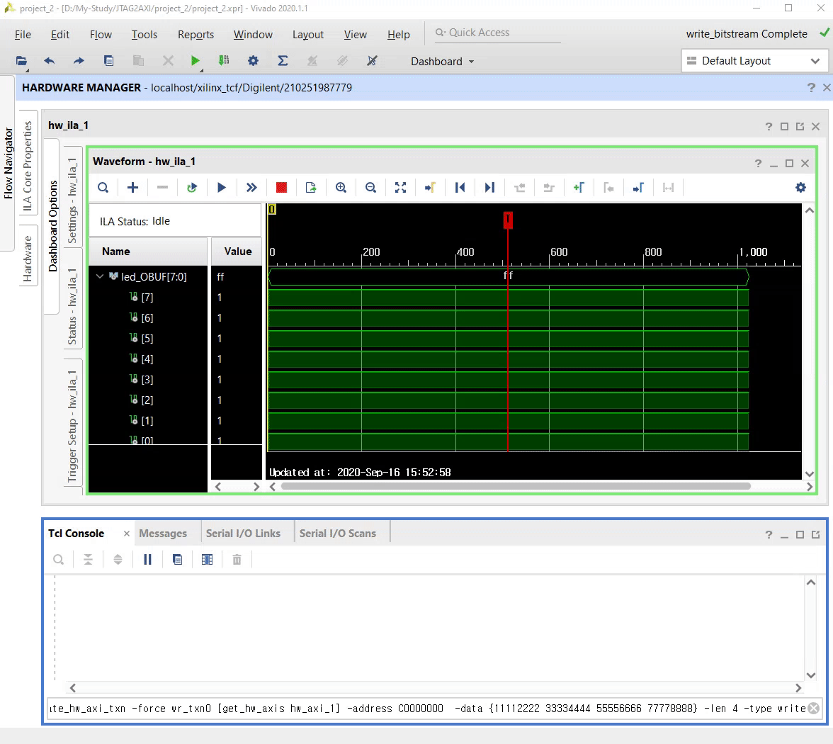
다음의 TCL command를 TCL console에 기입한 후, Enter합니다. (아래 Write2.txt 참조)
| TCL command (Write Operation) |
| create_hw_axi_txn -force wr_txn0 [get_hw_axis hw_axi_1] -address 40000000 -data {000000FF} -len 1 -type write run_hw_axi wr_txn0 |
이 후, 아래의 Animated GIF와 같이 Waveform 창에서 "Run trigger immediate for this ILA core" 아이콘을 클릭합니다.
Output pin인 led[7:0]="11111111"임을 확인할 수 있습니다.
Output pin인 led[7:0]="11111111"이므로 Board의 8개 LED 모두가 "on"됩니다.

4.
다음의 TCL command를 TCL console에 각각 기입한 후, Enter합니다.
| TCL command (Read Operation) |
| create_hw_axi_txn -force rd_txn0 [get_hw_axis hw_axi_1] -address 40000000 -len 1 -type read run_hw_axi rd_txn0 |
이 후, 아래의 Animated GIF와 같이 Address "0x40000000"의 Data를 Read하여 보여줍니다.
(TCL Console에서 "READ DATA is : 000000ff"을 확인할 수 있습니다.)

Step 6 : TCL command for write and read in the Console(2)
1.
JTAG-to-AXI Master IP를 지나서, AXI Interconect( or Smart Connect)를 지나 연결되어 있는 BRAM에 Write/Read를 하여 보겠습니다.
BRAM의 Base Address는 "0xC000_0000" 입니다.
2.
다음의 TCL command를 TCL console에 기입한 후, Enter합니다. (아래 Write_BRAM.txt 참조)
| TCL command (Write Operation) |
| create_hw_axi_txn -force wr_txn0 [get_hw_axis hw_axi_1] -address C0000000 -data {11112222 33334444 55556666 77778888} -len 4 -type write run_hw_axi wr_txn0 |
아래의 Animated GIF와 같이 ...
위 TCL command로 다음의 4가지 작업이 진행 됩니다.
- Address "0xC0000000"에 Data "0x11112222"를 write합니다.
- Address "0xC0000004"에 Data "0x33334444"를 write합니다.
- Address "0xC0000008"에 Data "0x55556666"를 write합니다.
- Address "0xC000000C"에 Data "0x77778888"를 write합니다.
3.
다음의 TCL command를 TCL console에 기입한 후, Enter합니다. (아래 Read_BRAM.txt 참조)
| TCL command (Read Operation) |
| create_hw_axi_txn -force rd_txn0 [get_hw_axis hw_axi_1] -address C0000000 -len 4 -type read run_hw_axi rd_txn0 |

지금까지 JTAG-to-AXI Master IP의 사용법에 대하여 알아보았습니다.
여러분의 FPGA 설계에 조금이라도 도움이 되었으면 합니다.
오늘도 좋은 하루 되세요.
(공감, 구독, 댓글은 저에게 힘이 됩니다!)
Create Date: September 16, 2020
Posted By: Mouessee
Xilinx 본사는 한국 내에 Corporate and Sales Distributor로 MAKUS를 두고 있습니다.
Xilinx 국내 Corporate and Sales Distributor인 MAKUS는 XIlinx FPGA Device를 기술영업을 통해 판매하며 기술지원이 가능합니다.
MAKUS www.makus.co.kr
관련 BLOG
------------------------------
------------------------------
Using the JTAG-to-AXI to test Peripherals on Artix-7 board (1/2)
Using the JTAG-to-AXI to test Peripherals on Artix-7 board (1/2)
Introduction JTAG to AXI Master (PG174 - October 5, 2016) 라는 IP를 사용하면, Vivado Hardware Debug Manager의 TCL console을 통하여 JTAG을 지나서, FPGA 내부 Design된 JTAG-to-AXI Master IP를 지나서,..
740280.tistory.com
Using the JTAG-to-AXI to test Peripherals on Artix-7 board (2/2)
Using the JTAG-to-AXI to test Peripherals on Artix-7 board (2/2)
Introduction 앞서 BLOG에서 JTAG to AXI Master (PG174 - February 4, 2021) 라는 IP를 사용하면, Vivado Hardware Debug Manager의 TCL console을 통하여 JTAG을 지나서, FPGA 내부에 Design된 JTAG-to-AXI..
740280.tistory.com
How to monitor XADC with "JTAG to AXI Master" IP
How to monitor XADC with "JTAG to AXI Master" IP
Introduction "JTAG to AXI Master" IP를 이용하여 XADC를 monitoring하는 방법에 대하여 설명하겠습니다. (여기서는 간단하게 XADC를 이용하여 FPGA Device의 온도(Temperature)를 monitoring 하겠습니다.) T..
740280.tistory.com
'Xilinx > Vivado' 카테고리의 다른 글
| How to monitor XADC with "JTAG to AXI Master" IP (0) | 2022.08.31 |
|---|---|
| Using the JTAG-to-AXI to test Peripherals on Artix-7 board (2/2) (0) | 2022.08.31 |
| How to install a Board Definition file (0) | 2022.08.16 |
| My recommended book for "VHDL" or "Verilog" users (0) | 2022.08.11 |
| ILA not triggering at 15 MHz (0) | 2022.08.07 |